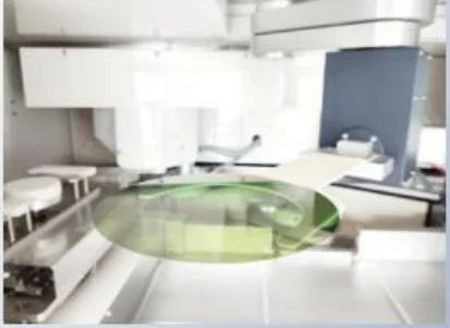
 SUBSTRATE / 01
4H-SiC wafers
N-type conductive and high-purity semi-insulating options. Diameter, thickness, off-axis, resistivity, defect limits and surface finish are matched to your process.
Review available specs ↗From high-purity crystal to production-ready wafer and growth equipment, source the SiC materials that move demanding power and RF designs forward.
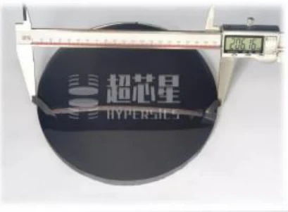 SUPPLIER REFERENCE / 4H-SiCWIDE
Silicon carbide (SiC) is a compound semiconductor whose wide bandgap, high critical electric field and high thermal conductivity make it valuable in high-voltage, high-temperature and high-frequency electronics.
Compared with conventional silicon, SiC devices can support higher voltage with lower conduction and switching losses in suitable designs. System results depend on device architecture, packaging, gate drive and thermal design—not material alone.
See where SiC fits ↗Illustrative material-level comparisons; values vary by reference, direction, temperature and method. Not a device performance guarantee.
We coordinate supplier-backed specifications and confirm the exact grade, availability and inspection criteria before quotation.
SUBSTRATE / 01N-type conductive and high-purity semi-insulating options. Diameter, thickness, off-axis, resistivity, defect limits and surface finish are matched to your process.
Review available specs ↗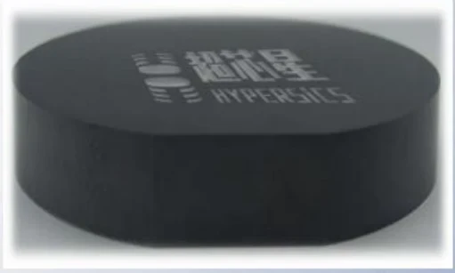 CRYSTAL / 02
Crystal formats for downstream slicing and substrate processes. Crystal quality, dimensions and electrical type require project confirmation.
Discuss boule requirements ↗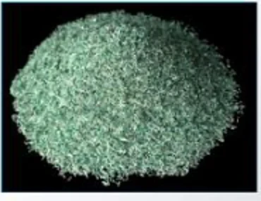 FEEDSTOCK / 03
Supplier datasheet lists conductive powder above 99.9999% purity with 8–20 and 20–40 mesh grades. Lot limits should be checked against its certificate.
Request powder data ↗Supplied equipment material includes a SiC crystal-growth furnace and platform plus an induction-heating power supply. Specific parameters are not stated and should be requested from the supplier.
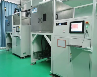 SUPPLIER REFERENCE IMAGE
Principle. In physical vapor transport (PVT), high-purity SiC source is heated in a controlled hot zone. Vapor species move along a temperature gradient to a cooler seed crystal, where material deposits and a boule grows.
Value. Furnace thermal-field design, pressure control, hot-zone materials and recipe discipline affect repeatability and crystal quality. The supplier states that mature process support may be included with furnace purchase; confirm scope, training and acceptance deliverables in writing.
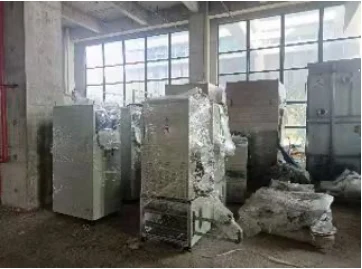 SUPPLIER REFERENCE IMAGE
Principle. Alternating current energizes an induction coil, creating a changing magnetic field. This induces current in a conductive susceptor or work zone, generating heat without direct contact from a resistance element.
Value. Induction can provide responsive, localized heating when matched to coil, susceptor and furnace control. Actual efficiency and uniformity depend on the complete system design.
Supplier material describes related crystal-growth, processing and inspection equipment and assistance with line setup. Machine list, facilities, performance and integration responsibility need project-level confirmation.
Plan an equipment line ↗SiC is selected when efficiency, voltage handling, switching frequency, heat and package size need to be balanced at system level.
Traction inverters, onboard chargers and DC-DC converters.
EVSolar inverters, wind converters and storage systems.
GRIDHigh-power fast chargers and efficient power modules.
CHARGEMotor drives, power supplies and high-temperature electronics.
INDUSTRYRF devices and infrastructure with demanding thermal needs.
RFValues below are transcribed from supplied supplier datasheets. Different documents describe different products and grade tables. They are not one guaranteed specification; final acceptance criteria belong in the purchase specification.
| Parameter | Supplier specification | Unit / note |
|---|---|---|
| Polytype | 4H | Crystal type |
| Diameter | 200 +0 / −0.2 | mm |
| Thickness | 500 ±25 | µm |
| Surface orientation | On-axis <0001>; off-axis 0 ±0.25 | degrees |
| Notch orientation | <1-100> ±1 | degrees |
| Warp | P ≤25 / R ≤35 / D ≤60 | µm; supplier grade columns |
| Bow | P ±15 / R ±25 / D ±40 | µm; supplier grade columns |
| TTV | P ≤5 / R ≤10 / D ≤15 | µm; supplier grade columns |
| Micropipe density | P ≤1 / R ≤5 / D ≤15 | cm⁻²; supplier grade columns |
| Si-face roughness | Ra ≤0.2 | nm, 10×10 µm area |
| Resistivity | P ≥1×10⁸; R 100% area >1×10⁵; D 70% area >1×10⁵ | Ω·cm; grade definitions apply |
| Metal impurities | ≤5×10¹⁰ | Measurement basis to confirm |
| Parameter | Supplier datasheet range / value | Unit / note |
|---|---|---|
| Polytype | 4H | Common power-device polytype |
| Diameters listed | 150 and 200 | mm; separate product tables |
| Thickness listed | 350±25 or 500±25 | µm; product-dependent |
| Off-orientation | 4° toward [11-20] ±0.5° | degrees; listed wafer grade |
| Resistivity | 0.015–0.028 | Ω·cm; one 8-inch table |
| Si-face roughness | <0.2 | nm; one product table |
| Warp / bow / TTV | Grade-specific; examples include warp ≤40 µm and TTV ≤10 µm | Do not compare across grade tables |
| Defect metrics | Micropipe, TSD, TED, BPD vary by grade | Request exact revision / grade |
| Parameter | Supplier specification | Unit / note |
|---|---|---|
| Product type | High-purity conductive SiC powder | Feedstock |
| Purity | >99.9999% | Confirm method and lot certificate |
| Particle size | 8–20 / 20–40 | mesh |
| Appearance | Yellow-green | As stated in supplier sheet |
| Trace elements | Examples: Li, K, Ni, Ca, Ti, Fe <0.05 ppm wt; B, Cl <0.5 ppm wt; Al <0.2 ppm wt | See full element list in source specification |
Request the exact current revision and lot-specific certificate before procurement. N-type values summarize separate supplier tables and must not be mixed.
SiC is not automatically right for every circuit. Where its properties fit the design, it can enable benefits that conventional silicon may struggle to deliver at the same voltage and temperature.
Its high critical electric field can enable thinner, more heavily doped drift regions for a given blocking-voltage class, helping reduce conduction losses in suitable structures.
High thermal conductivity can help conduct heat away from active regions. Package, cooling and interface design remain essential.
SiC devices can switch quickly with low losses when device and gate-drive design are tuned together.
Substrate and device cost, gate drive, EMI control and reliability qualification belong in total-cost analysis. Let your use case guide the choice.
Tell us the device, process stage and target values. Xinkehui can coordinate supplier options for substrates, boules, powder or growth equipment and confirm which requirements are achievable before you commit.
Start a specification review ↗
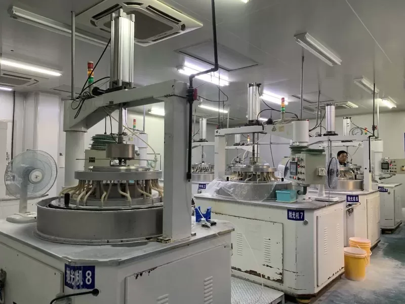
Xinkehui’s official company profile describes the business as a semiconductor-materials supplier established in 2016, serving customers in more than 50 countries and regions, with production bases in Wuhan and Wuxi and in-house R&D centers. These are company-published profile statements.
The facility image shown here is an architectural rendering published by Xinkehui, not a current factory photograph. The adjacent production-equipment image is also from the official company website. For this SiC project, the supplied product and equipment brochures identify HyperSiCs / 超芯星 as the source of the referenced SiC products and equipment; supplier claims remain separate from Xinkehui’s profile.
Sample availability, freight, replacement and return conditions are confirmed per item and order before purchase. No blanket free-sample, free-shipping or free-return promise is made here.
Map targets against current supplier data and clarify grade definitions.
Confirm sample size, cost, freight and qualification documents.
Confirm packing, inspection records, lead time and shipment terms.
Report concerns with order reference and inspection evidence for review.
Start with your use case, then share exact requirements with the team.
SiC is a wide-bandgap compound semiconductor made from silicon and carbon. Its properties support power and RF devices that handle demanding voltage, switching or temperature conditions.
N-type substrates are conductive through donor doping and are commonly used for vertical power-device epitaxy. High-purity semi-insulating substrates have much higher resistivity and are often considered for RF or isolation-sensitive structures.
The supplied substrate specifications list 4H-SiC. Confirm the polytype and grade on the current product datasheet.
Yes. The supplied materials include 150 mm and 200 mm wafer tables, including an 8-inch semi-insulating specification. Availability and grade require confirmation.
We can submit targets to the relevant supplier and confirm feasible options. Customization depends on crystal, process, yield and order constraints and is not assumed until confirmed.
Include diameter, thickness, polytype, conductivity type or resistivity, orientation/off-axis, surface finish, warp/bow/TTV, defect limits, packaging and inspection documents.
Warp describes overall wafer shape deviation; bow describes center displacement relative to the surface reference; TTV is the difference between maximum and minimum thickness across a defined area.
A common bulk-growth method is physical vapor transport. Source material sublimes in a hot zone, then vapor species move along a temperature gradient to a cooler seed crystal and grow. Confirm the actual furnace configuration and supported process with the supplier.
It drives alternating current through an induction coil. The magnetic field induces heating in a conductive susceptor or work zone. The supply must be matched to the coil, furnace and control design.
The supplier brochure says a mature growth process may be included with a furnace purchase. Confirm scope, training, transfer documents, commissioning and acceptance terms in the quotation.
Supplier material describes related growth, processing and inspection equipment plus line setup assistance. Machine list, facilities and integration responsibilities need confirmation.
Sample availability, cost and freight depend on product, format, destination and purpose. Request written terms for your specific inquiry.
Eligibility depends on the quotation, purchase specification, inspection method and supplier terms. Agree conditions before ordering.
Ask which lot documents are available, such as certificate of analysis, inspection data, packing list and traceability records. Confirm the exact set before order.
Send your target spec and application. We’ll help frame the next supplier conversation.